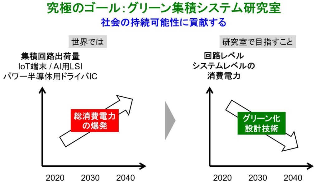
The ultimate goal of my laboratory is to contribute to the sustainability of society. The shipment volume of integrated circuits, such as IoT devices, AI LSIs, and driver ICs for power semiconductors, has been increasing year by year. Proportionally, the total power consumption of integrated circuits is also increasing. To ensure societal sustainability, this increase must be controlled. Therefore, in my laboratory, we are conducting research and development on “greening design technology” to reduce power consumption at both the circuit level and system level.
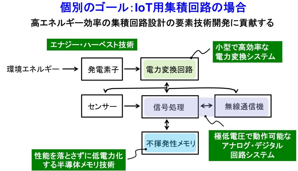
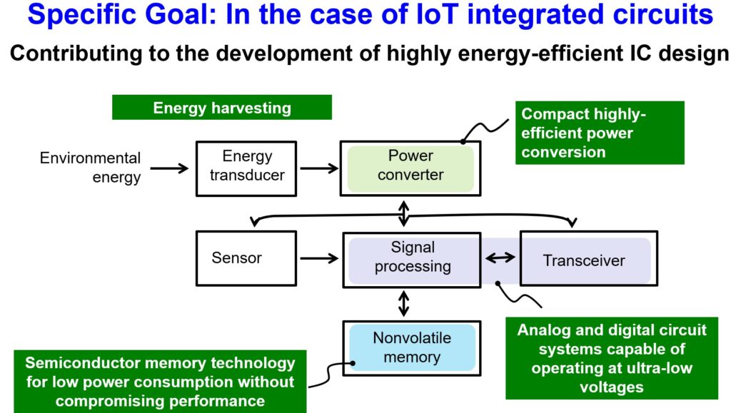
Here is an explanation of integrated circuits for IoT applications. Sensors monitor environmental temperature variations and vibration conditions, and the results are stored in non-volatile memory. Information is periodically sent to and received from the cloud via a wireless communication device. In locations without access to commercial power sources, energy harvesting devices are used to convert environmental energy into electricity instead of relying on batteries. The power obtained from the energy harvesting devices is supplied to the sensor module through a power conversion circuit. The parts written in green indicate “elemental technologies for high-energy-efficient integrated circuit design”, and by contributing to their development, we aim to “contribute to the sustainability of society”.
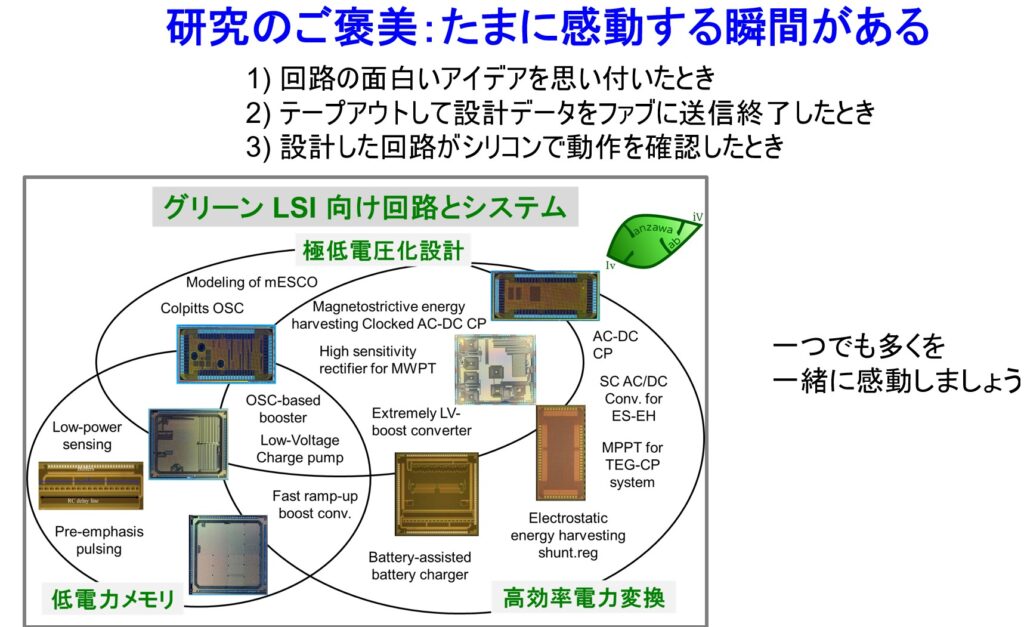
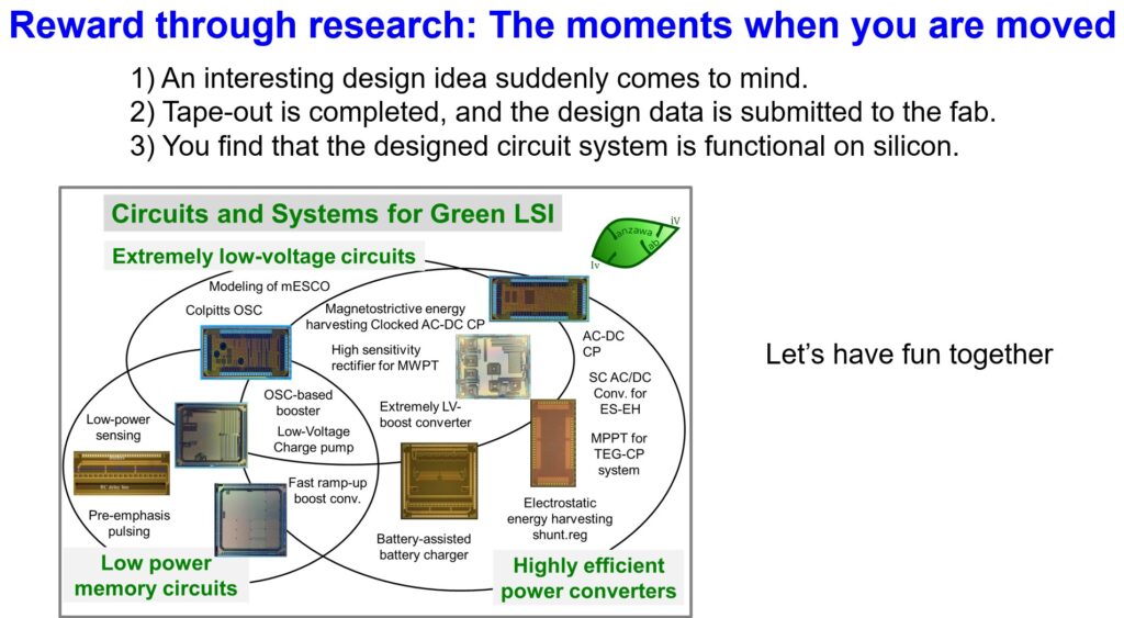
The reward through research is the occasional moments of inspiration and excitement. For example, when you come up with an interesting circuit idea. If, after reviewing past literature, you find that the idea is novel, it can become the basis for a patent or a research paper. When you turn that idea into an actual circuit design and send the design data to the fabrication facility, the design phase comes to an end. At that moment, you feel a sense of accomplishment, like “I did it!”. When you measure the circuit you designed yourself and confirm that it works on silicon, you can’t help but say, “Yes!” out loud. Experiencing such moments of excitement from time to time makes you realize, “Research is fun.” I hope the students in my laboratory can experience as many of these moments of inspiration and excitement as possible.
(Topics) Energy harvesting technology Semiconductor memory system Analog circuit system Power conversion system
The shipment volume of integrated circuits, such as IoT devices, AI-specific LSIs, and driver ICs for power semiconductors, continues to expand every year. As a result, the overall power consumption of integrated circuits is also consistently increasing. Low power consumption at both the circuit and system levels, in other words, greening, is becoming increasingly important. In our research laboratory, we are conducting research and development on technologies to green the circuit systems of digital, analog, memory, and power converter used in these LSIs.
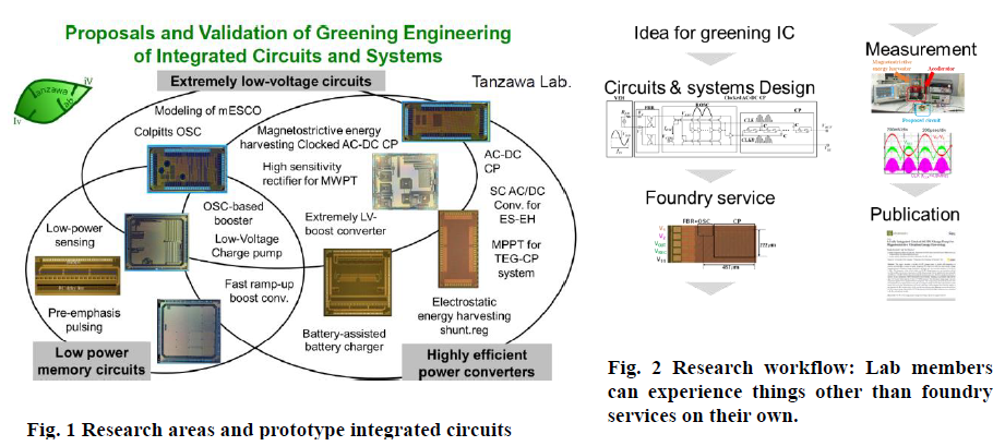
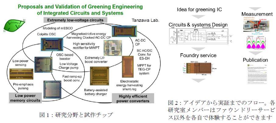
Each lab member will have the opportunity to gain experience in circuit design (creating circuit diagrams, verifying operation with a circuit simulator, and designing layouts) as well as in the measurement and evaluation of prototype circuits and paper writing, as shown in Figs. 1, 2.
Let’s enjoy imagining circuit operation in a physical sense, quantifying characteristics with mathematical sense, and contemplating the greening of the system through overall optimization. If you are confident that you can continue what you are working on, you can do well enough in this laboratory.
Integrated Systems Field, Greening Integrated Systems Laboratory, Tel: 093-692-5349, E-mail: toru.tanzawa at waseda.jp URL: http://tanzawa-lab.w.waseda.jp/
Toru Tanzawa is a professor in the Graduate School of Information, Production and Systems at Waseda University. He pursues the Greening of integrated circuits and systems from a circuit design perspective. He has been engaged in research and development of memory, analog, and power circuits at Toshiba and Micron for 25 years and at Shizuoka university for seven years. Dr. Tanzawa holds 280 U.S. patents and has published 60 papers in IEEE conferences and journals. Toru Tanzawa is a Fellow of IEEE. He is included in the world’s top 2% of top scientists [1]. He received the B.S. degree in physics from Saitama University, Saitama, Japan, in 1990, the M.S. degree in physics from Tohoku University, Sendai, Japan, in 1992, and the Ph.D. degree in electrical engineering from The University of Tokyo, Tokyo, Japan, in 2002.
[1] Ioannidis, John P.A. (2025), “August 2025 data-update for “Updated science-wide author databases of standardized citation indicators””, Elsevier Data Repository, V8, doi: 10.17632/btchxktzyw.8: https://elsevier.digitalcommonsdata.com/datasets/btchxktzyw/8